Engineering-led review
Composition, purity, geometry, process and documentation are reviewed before quotation.
 Request a Quote
 Established 2013 · Türkiye · Europe
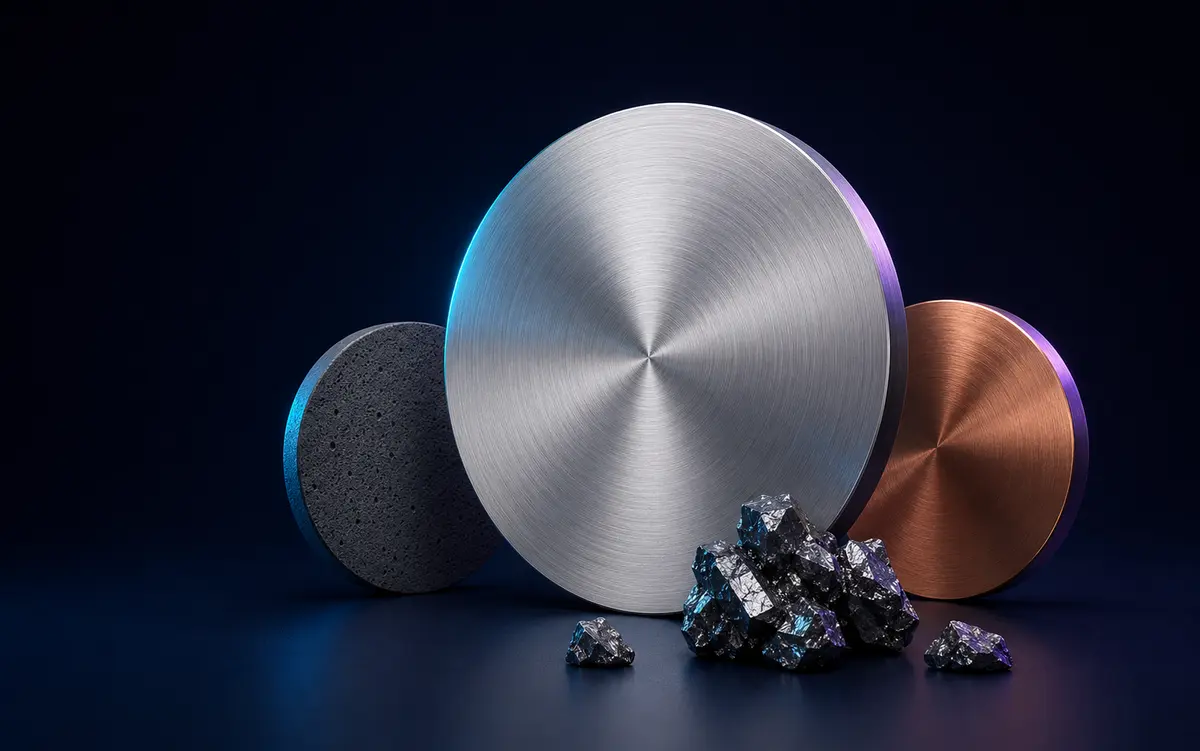
An engineering-led advanced materials supplier coordinating technical evaluation, qualified production and international delivery of targets, evaporation sources, rare earths, ceramics and semiconductor substrates.
Targets Evaporation Rare Earths Wafers Technical Ceramics
 SPUTTERING TARGET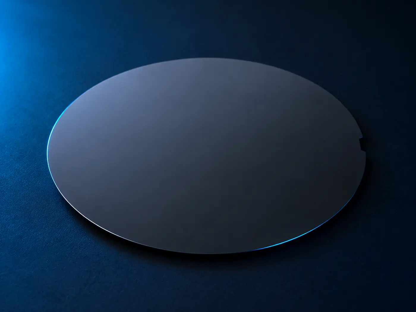
N-type, semi-insulating and epi-ready substrate options.
Explore family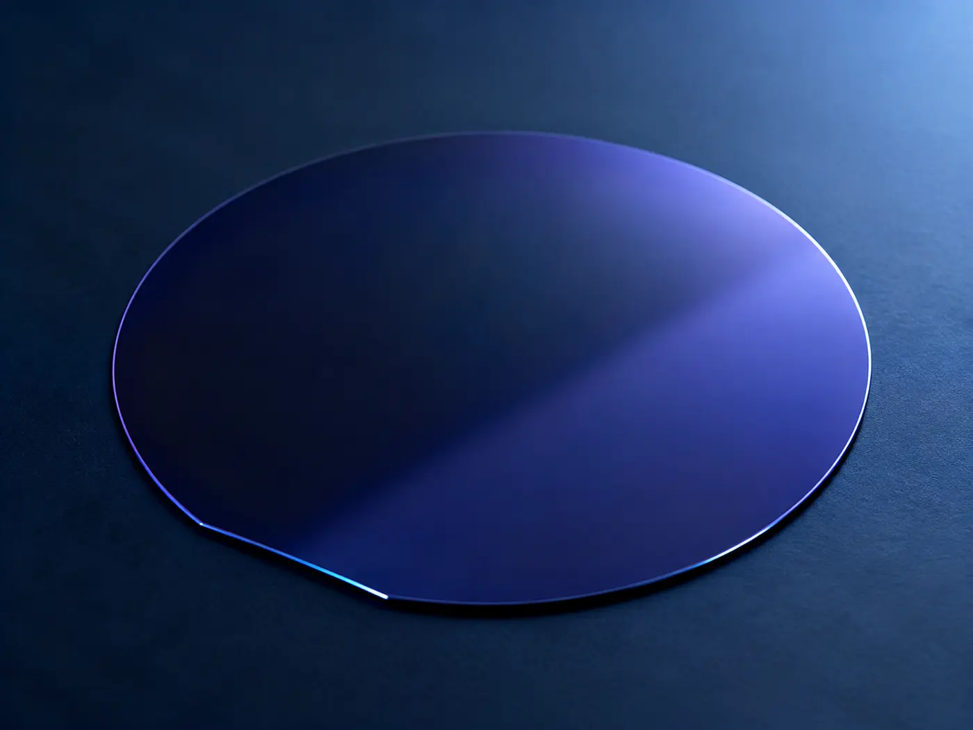
Bulk wafers, templates and epitaxial structures by specification.
Explore family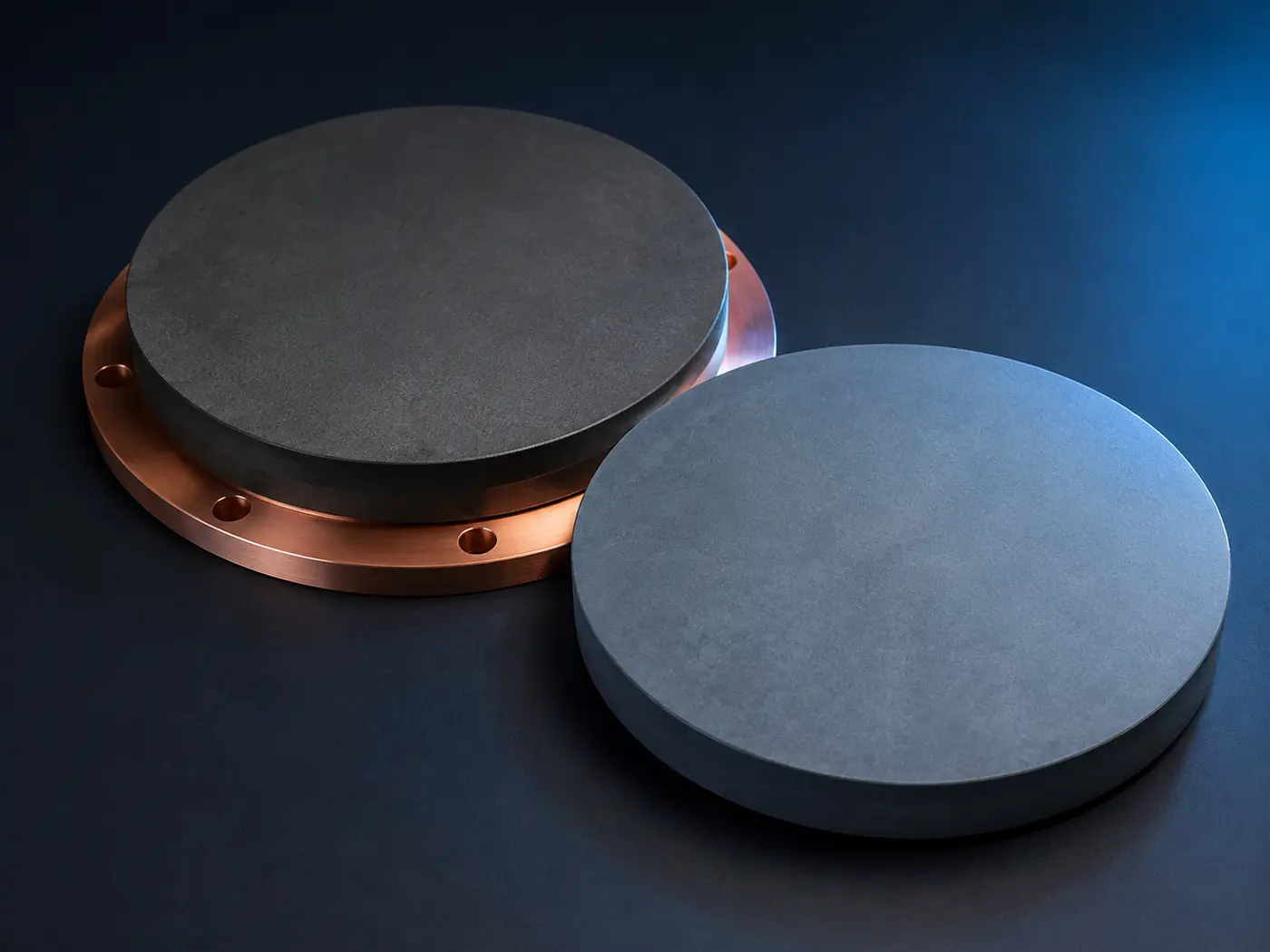
Ceramic sputtering targets for display, photovoltaic and optoelectronic films.
Explore family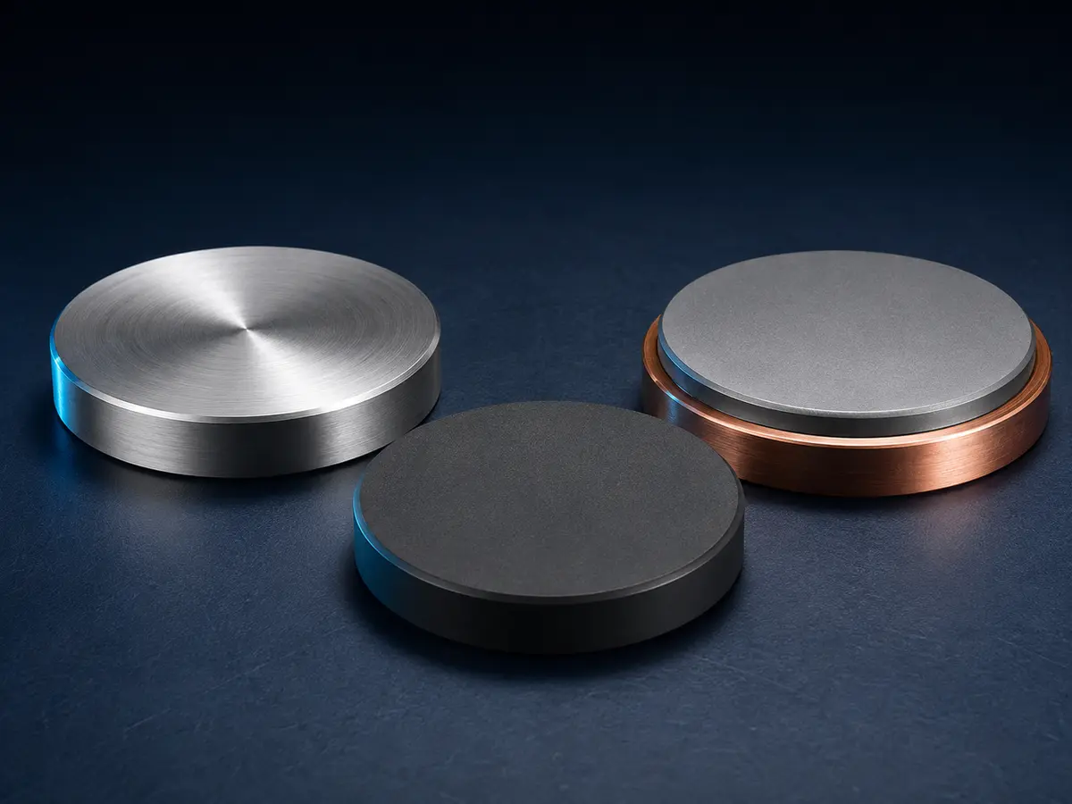
Custom scandium content and dimensions for advanced piezoelectric films.
Explore family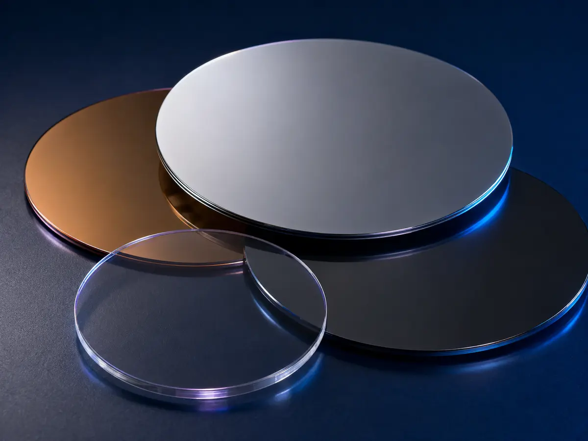
Bulk and thin-film bonded wafers for photonic device research.
Explore family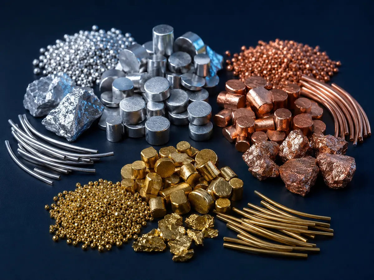
Sputtering targets and evaporation pellets in high-purity grades.
Explore familyDoped, undoped and semi-insulating epi-ready substrates.
Explore family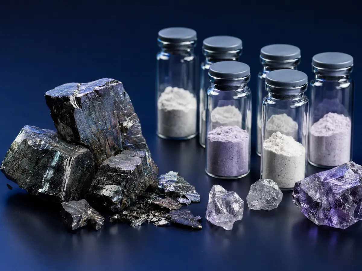
Rare-earth metal pieces, ingots and oxide powders for magnetic and advanced research.
Explore family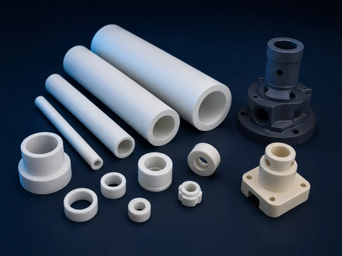
Tubes, insulators, wear parts and drawing-based precision components.
Explore familyMaterial portfolio
Our product pages show popular examples, not a closed catalogue. We review metals, alloys, ceramics, compounds, powders, crystals and substrates around chemistry, purity, geometry and process.
Elemental metals, precious metals, alloys, oxides, nitrides, carbides, chalcogenides and custom multi-element compositions.
ITO · AZO · AlScN · CIGS · IZO · HfO₂ · Ta · W · CoFeB · YSZ + MOREExplore product rangeA broad range of metals, optical compounds and specialty materials in pellets, granules, pieces, slugs, wire and custom forms.
Au · Ag · Al · Cr · Cu · HfO₂ · MgF₂ · SiO₂ · Ta₂O₅ · ZnS + MOREExplore product rangeRare-earth metals, oxides, fluorides and custom compounds covering light, medium and heavy rare-earth families.
Nd · Pr · Dy · Tb · Gd · Sm · Y · Sc · Er · Yb · OXIDES + MOREExplore product rangeElemental, III–V, wide-bandgap, optical and functional oxide substrates for research through device development.
Si · SOI · SiC · GaN · GaAs · InP · GaSb · TFLN · LiTaO₃ · Sapphire + MOREExplore product rangeOxide and non-oxide ceramic tubes, plates, insulators, wear parts and drawing-based precision components.
Al₂O₃ · ZrO₂ · Si₃N₄ · AlN · SiC · BN · ZTA + MOREExplore product rangeWhy Adesis
Adesis helps turn a research or production requirement into a clearly specified, commercially deliverable material.
Learn about AdesisComposition, purity, geometry, process and documentation are reviewed before quotation.
Non-standard dimensions, doped compositions, backing plates, bonding and specialty forms are evaluated individually.
Since 2013, we have supplied targets and wafers from Türkiye to companies and universities across multiple European countries.
One technical and commercial contact follows specification, analysis documentation, packaging and DAP or EXW delivery.
Engineering-led sourcing
Material, purity, geometry, quantity and process conditions.
Technical feasibility, documentation and manufacturing route.
Order confirmation, controlled packaging and delivery.
Selected supply experience
Representative, anonymized examples from Adesis's target and wafer supply experience. Customer identities remain confidential.
Customer-defined composition and target geometry for photovoltaic thin-film research.
ZnO and TiO₂ target requirements reviewed with copper backing plates, purity and dimensional definition.
GaAs, GaSb and InP wafer supply for European university laboratories and advanced-technology companies.
Targets, evaporation materials and wafers consolidated around project-specific technical requirements.
Quality by specification
Applications
Technical knowledge
Practical notes prepared to help laboratories and purchasing teams define composition, geometry, surface, bonding and documentation before quotation.
View all technical notesTechnical inquiry
Send the material, purity, dimensions, quantity and application. We will review the complete specification before quoting.